
Editor-reviewed by Ahmad Zaidi based on analysis by TransforML's proprietary AI
CEO, TransforML Platforms Inc. | Former Partner, McKinsey & Company
What are the competing strategies of Applied Materials, Lam Research, and KLA for building 3D semiconductors and advanced packaging?
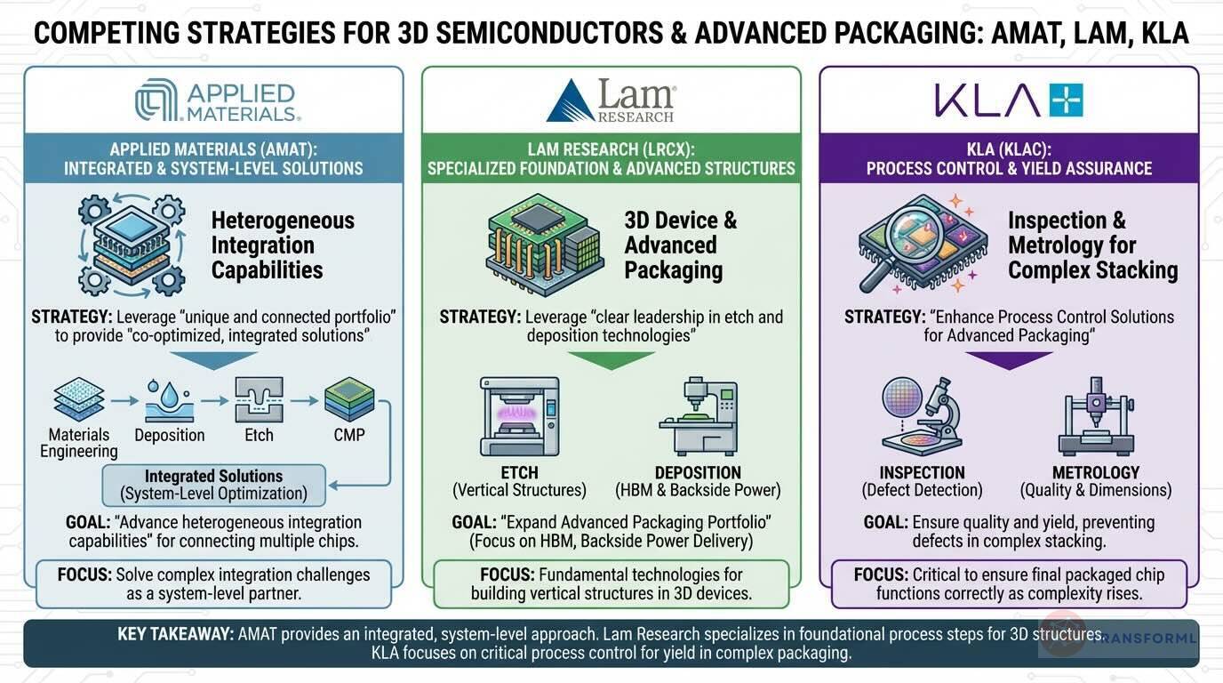
Advanced packaging and 3D semiconductors are the key to overcoming the limits of traditional chip scaling, and all three equipment leaders have distinct strategies to win in this critical market. Applied Materials pursues an integrated strategy, leveraging its "unique and connected portfolio" to provide "co-optimized, integrated solutions." Their goal is to "Advance heterogeneous integration capabilities," allowing customers to connect multiple chips together in a single package. This approach positions AMAT as a system-level partner that can solve complex integration challenges by optimizing across different process equipment.
In contrast, Lam Research and KLA focus on their specialized domains. Lam Research leverages its "clear leadership in the etch and deposition technologies" which are fundamental to building vertical structures in 3D devices. Their strategy is to "Expand Advanced Packaging Portfolio" with a specific focus on technologies like High-Bandwidth Memory (HBM) and enabling key architectural shifts like "backside power delivery." KLA, as the process control leader, focuses on ensuring quality and yield. Their strategy is to "Enhance Process Control Solutions for Advanced Packaging," as the complexity of stacking and connecting multiple die makes their inspection and metrology tools more critical than ever to prevent defects and ensure the final packaged chip functions correctly.
Review detailed strategy and competitive analysis of companies in Semiconductor-Equipment Makers
Source and Disclaimer: This article is based on analysis of Annual reports and other publicly available information. For informational purposes only (not investment, legal, or professional advice). Provided 'as is' without warranties. Trademarks and company names belong to their respective owners.